Physical Bands
Physical spectral response channels

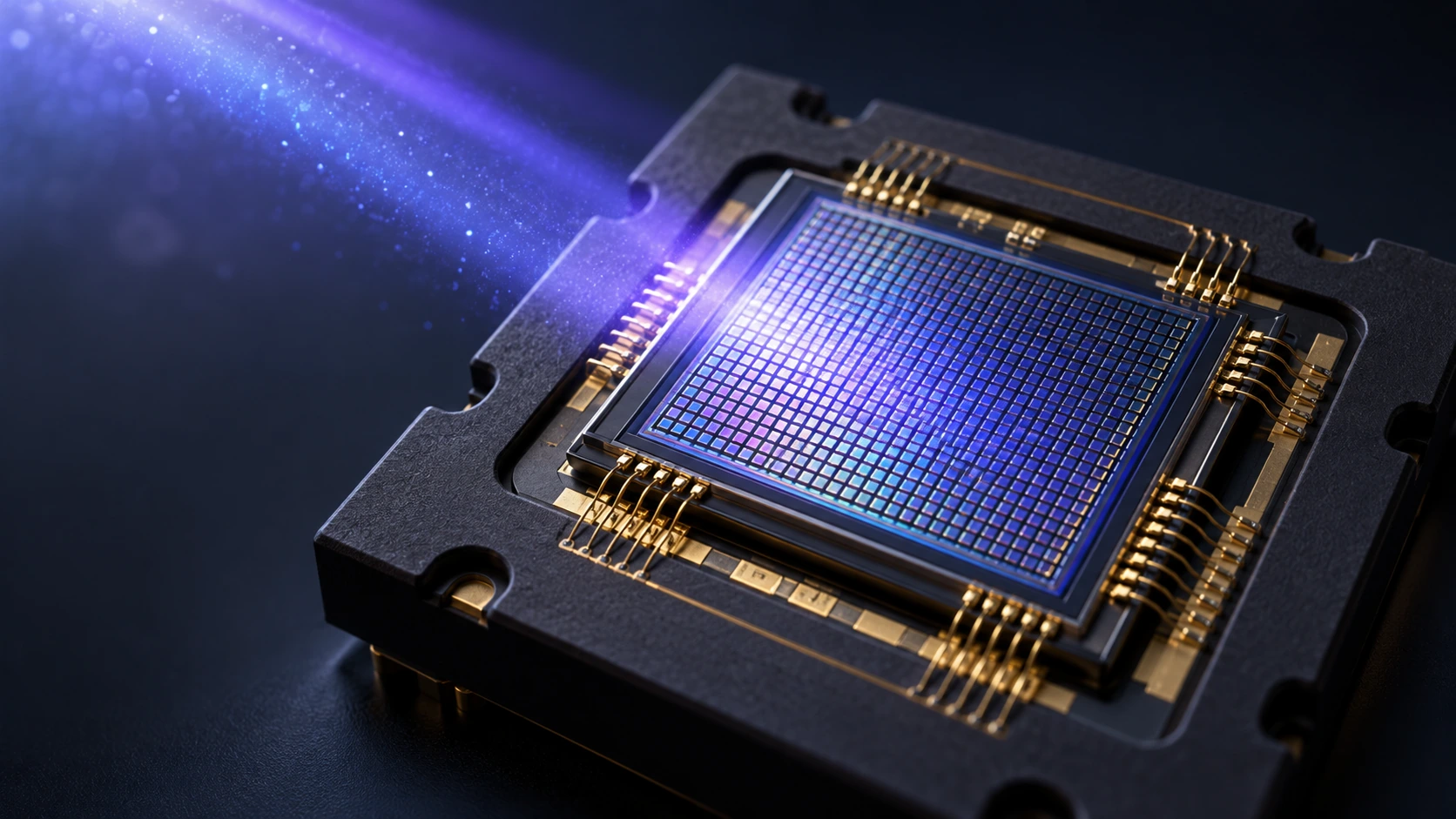
SPECTRAL SENSOR
Integrate calibration, acquisition and models for water spectroscopy, feature recognition and instrument front ends.
DETECTOR / CORE SPECIFICATIONS
Physical spectral response channels
Up to 120 output bands
Down to 1 nm
Time between consecutive samples
| Parameter | Visible | Near-Infrared |
|---|---|---|
| Documented Wavelength Coverage | 380–1000 nm | 1000–2400 nm |
| Physical Bands | 16 physical bands; defined separately from reconstructed output bands | |
| Reconstruction Capability | Up to 120 reconstructed bands; reconstructed spectral resolution down to 1 nm | |
| Temporal Sampling | Minimum sampling interval 10 ms; this is not end-to-end latency including transmission, reconstruction and display | |
| System Output | Channel signals, reconstructed spectra and image-analysis results depending on configuration | |
| Calibration | System calibration using the light source, reference spectra, detector response and actual optical path | |
Core capabilities supplied by the company: 16 physical bands, up to 120 reconstructed bands, reconstructed resolution down to 1 nm and minimum sampling interval 10 ms. Operating range, speed, resolution and simultaneous performance depend on configuration and testing. Complete instruments retain their individual specification tables.
SENSOR INTEGRATION
Select illumination, working distance and acquisition method for the target and its spectral features.
Define dark-field, reference-spectrum, thermal-drift and data-output requirements.
Calibrate spectra and validate reconstruction and inversion models using samples and application conditions.
Device models, packaging, interfaces and complete specifications are confirmed for the selected solution.
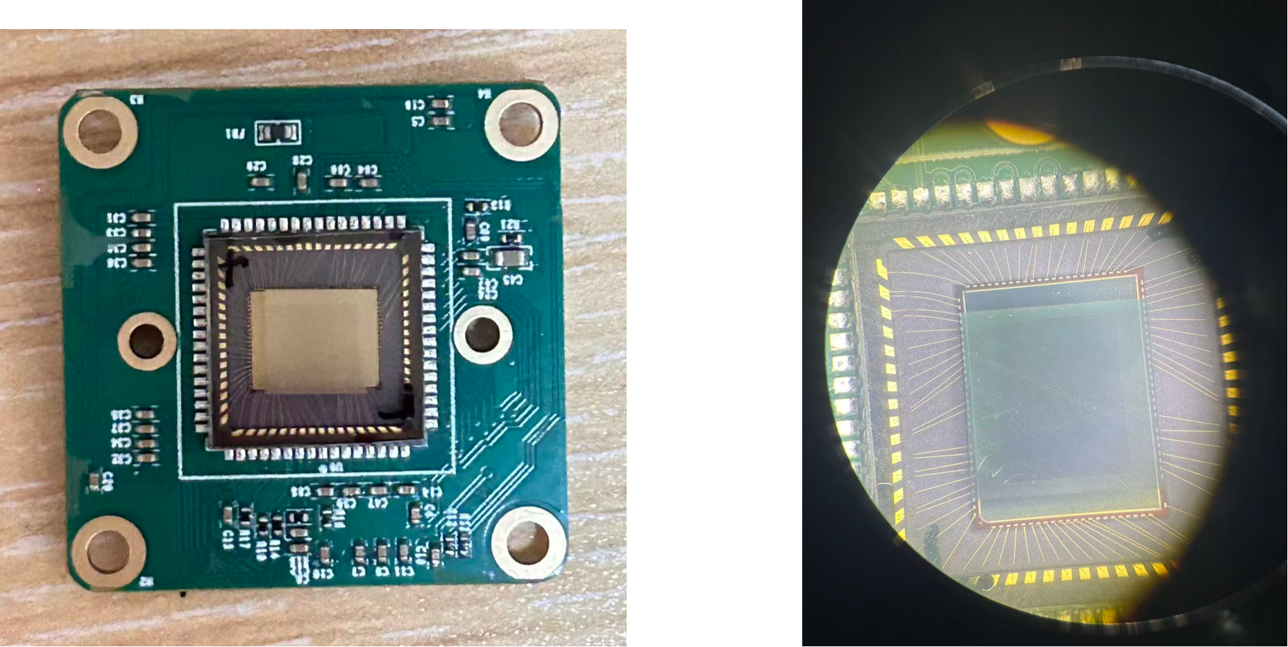
CAMERA MODULE
Camera module and chip photographs
CONTACT
Contact us for product selection, development
and project collaboration.
266 Fangzheng Avenue, High-tech Park, Liangjiang New Area, Chongqing, China
Zhongke Yaoguang (Chongqing) Optoelectronics Technology Co., Ltd.RESEARCH FOUNDATION