STEP 01
Spectral Calibration
Reference sources and instruments measure channel responses to relate wavelength, intensity and channel signals.

TECHNOLOGY
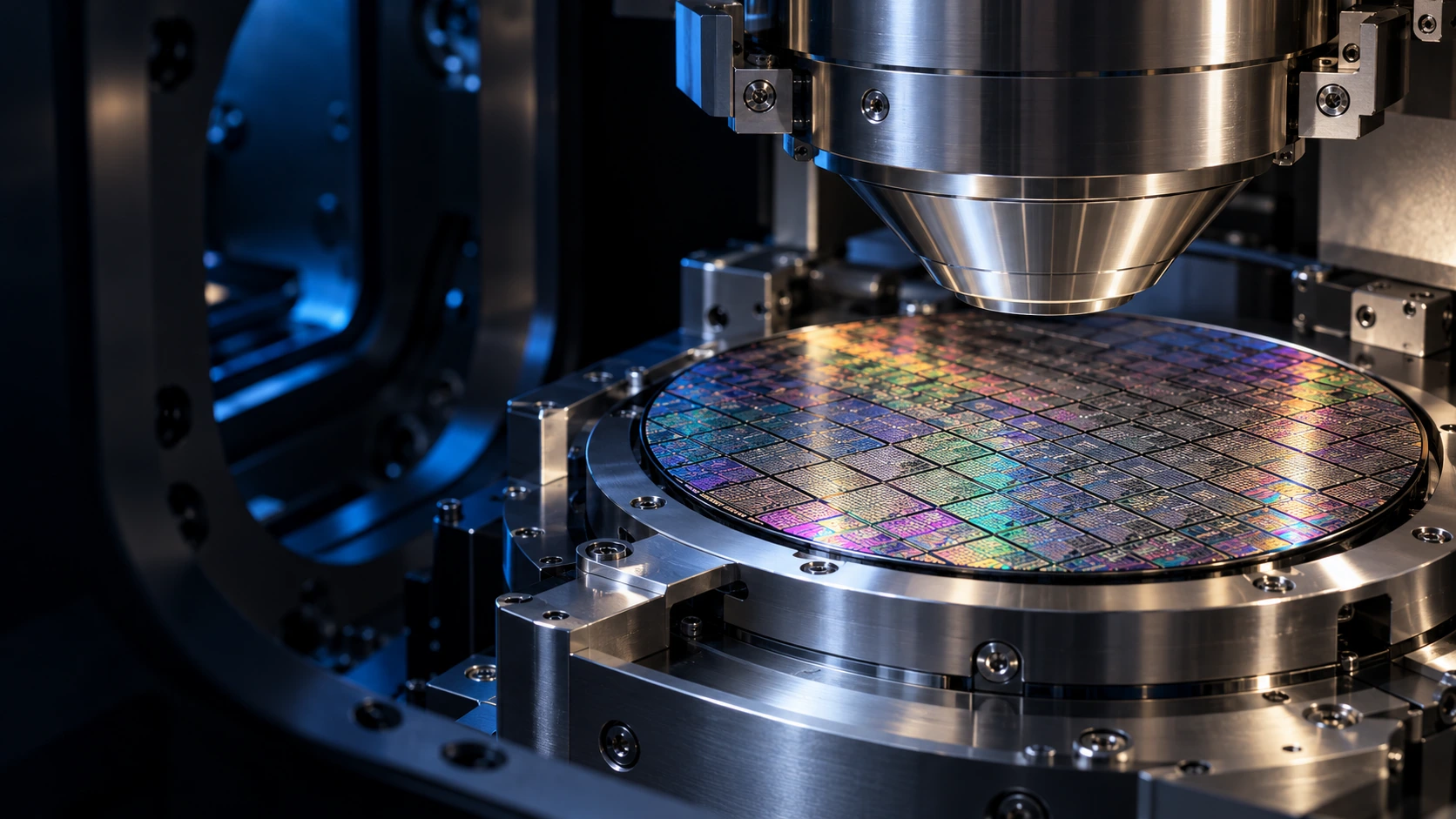
Simulation, micro/nano research and application validation for optical acquisition, control and transmission.
SPECTRAL COMPUTING / ALGORITHM CHAIN
Physical channels acquire encoded signals. Calibration and reconstruction recover spectral information, while recognition and inversion connect it to applications.
Reference sources and instruments measure channel responses to relate wavelength, intensity and channel signals.
Reconstruct up to 120 bands from 16 physical-channel responses, with resolution and stability evaluated against reference spectra.
Combine spatial texture and spectral features for classification, region recognition and anomaly detection, retaining images for verification.
Build models using target characteristics, reference measurements and project samples; estimate parameters and evaluate application scope.
METASURFACE / EXPERIMENTAL RESULTS
Metasurface samples, micro/nanostructure characterization and module spectral-imaging tests.
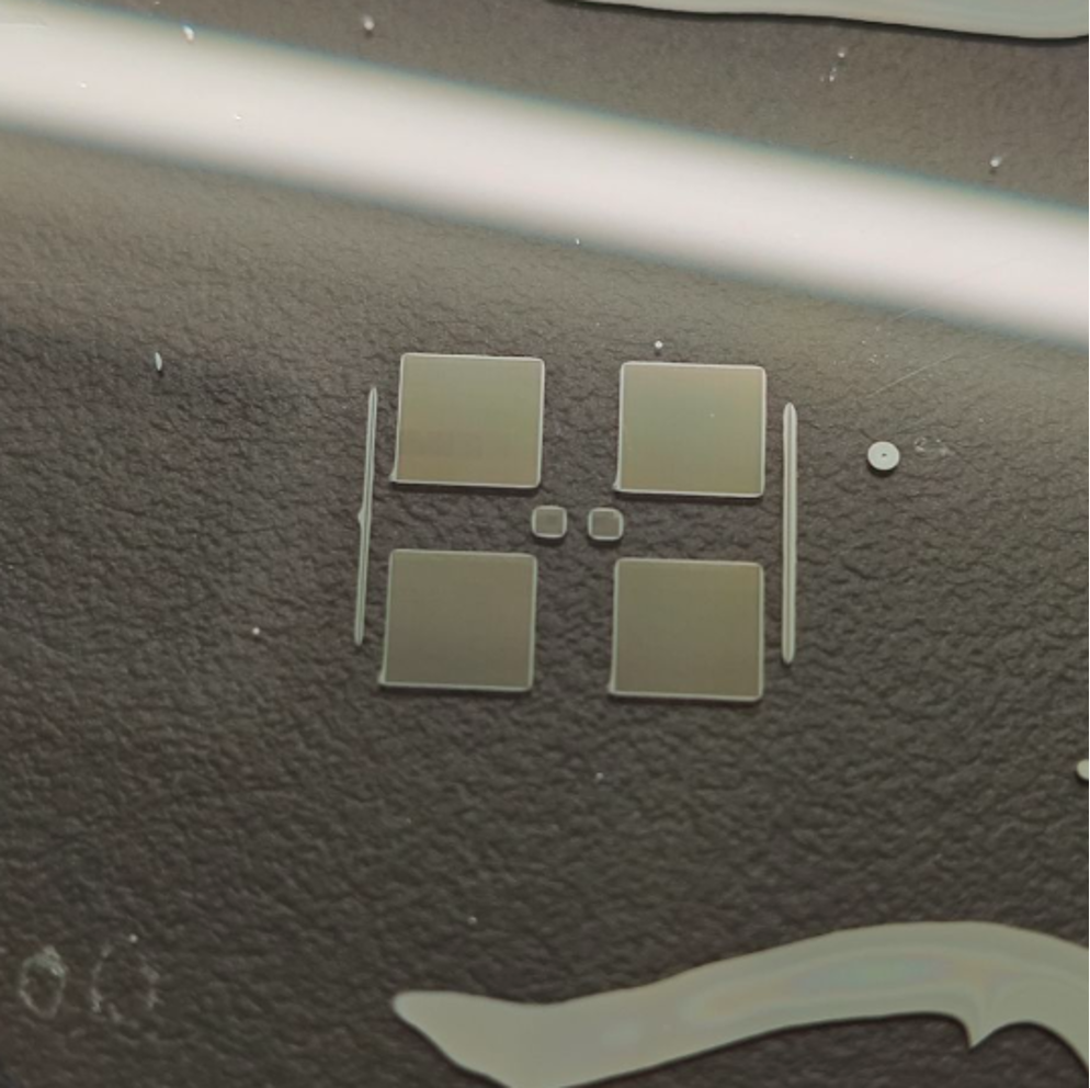
Physical samples and structural forms.
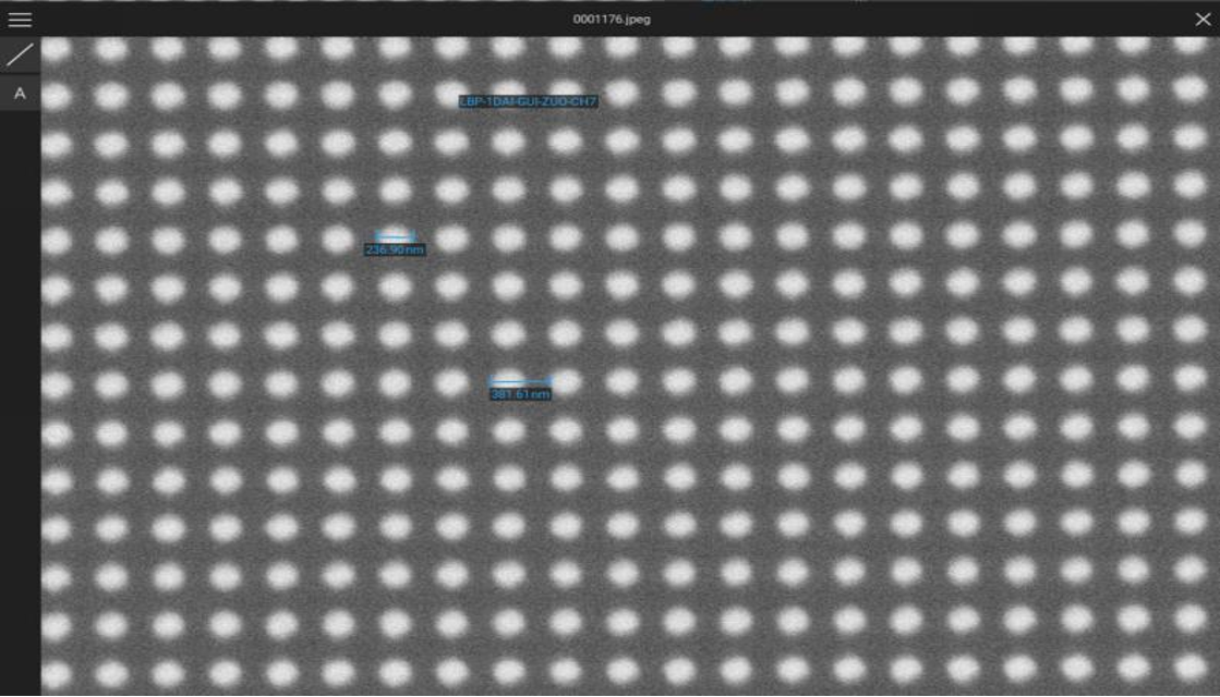
SEM characterization of metasurface arrays.
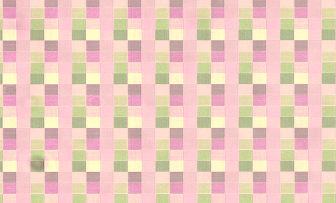
Microscopy of different unit-cell regions.
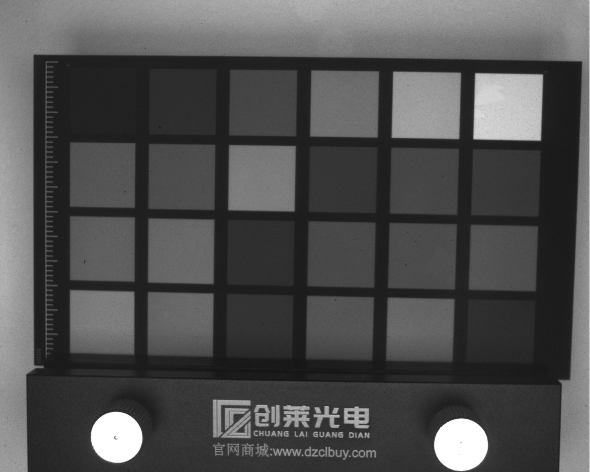
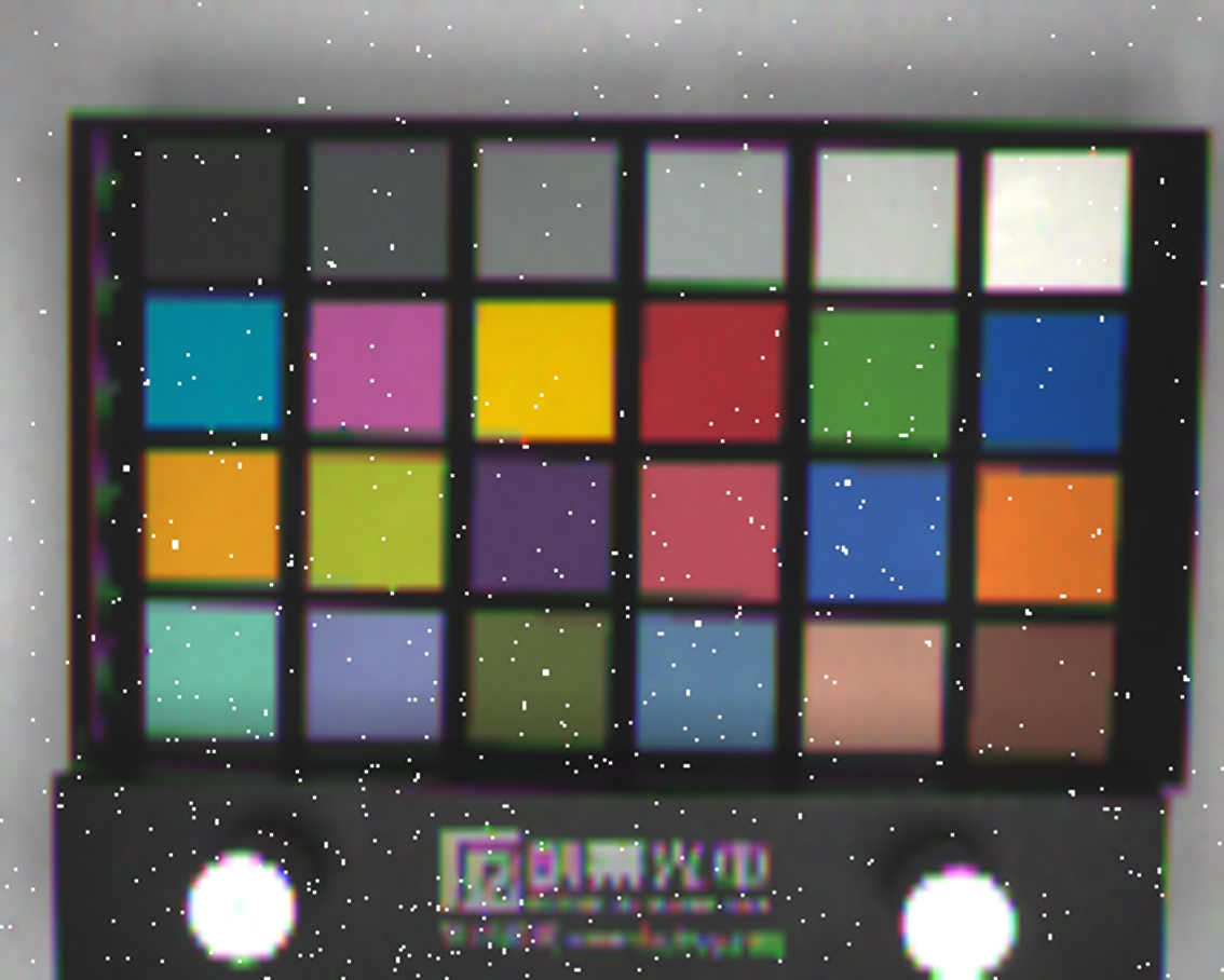
Compare monochrome-module images with spectral recovery after metasurface integration.
METASURFACE OPTICS / DESIGN TO TEST
Design planar microlens phase profiles and optical paths for the target band, numerical aperture and working distance.
Translate unit-cell and array layouts into fabrication using EBL, imprinting and supporting processes.
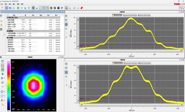
Optical microscopy, SEM and spot measurements assess geometry, focus position and energy distribution.
Compare actual inputs, receivers and reference paths to evaluate coupling efficiency, insertion loss and alignment sensitivity.
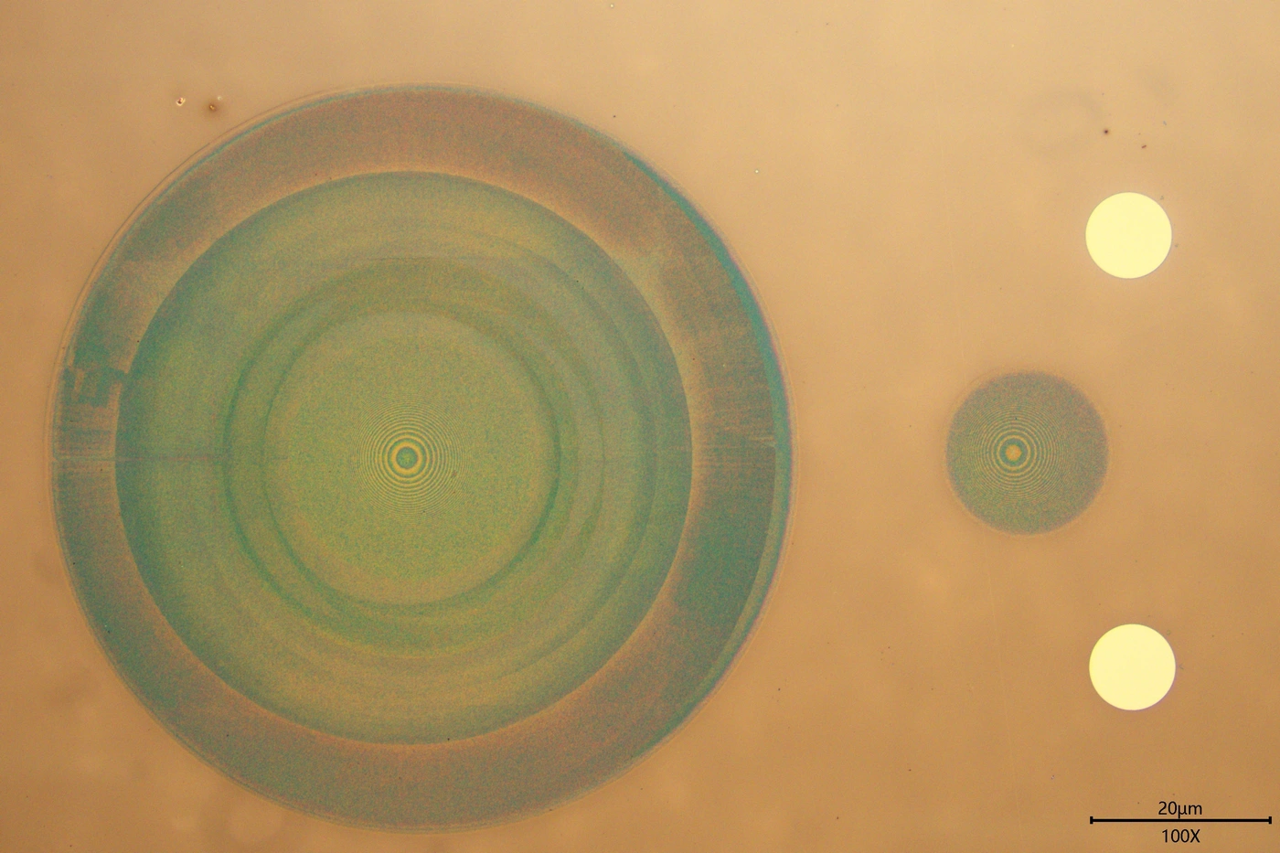
Sample insertion loss: 0.75 dB, for the reported sample, test optical path and alignment conditions.
04 / DEVICE & SYSTEM CO-DESIGN
Optical structures, signal conversion and electronic readout jointly determine equipment performance.
Co-design for the operating band, signal intensity and interface requirements.
Define incidence conditions and target signals
Structure response and optical field control
Electronic signal chains and evaluation methods
06 / TECHNOLOGY FOUNDATION
Building on simulation and EBL facilities,
we work with industry partners on design, fabrication and testing.
Micro/nanostructure modeling, optical response simulation and parameter optimization.
Electron-beam patterning and sample development using suitable materials and supporting fabrication processes.
Material selection, fabrication processes and optoelectronic interface integration with process and packaging partners.
Agree on test conditions, metrics and evaluation methods to guide the next iteration.
Materials, fabrication scope and supporting processes are confirmed for each project.
CONTACT
Contact us for product selection, development
and project collaboration.
266 Fangzheng Avenue, High-tech Park, Liangjiang New Area, Chongqing, China
Zhongke Yaoguang (Chongqing) Optoelectronics Technology Co., Ltd.RESEARCH FOUNDATION