01Materials Preparation
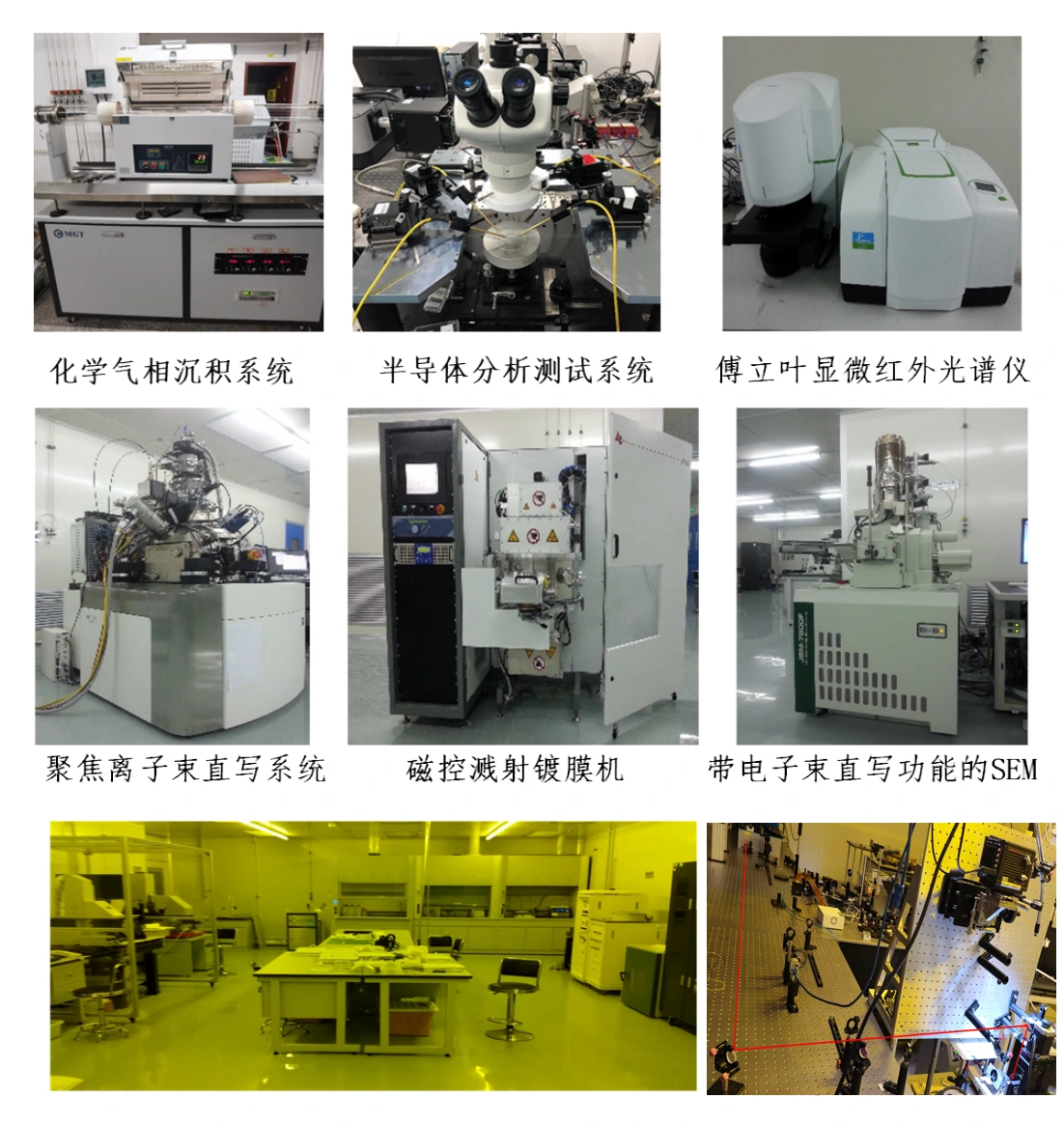
Chemical Vapor Deposition System
Material growth and thin-film preparation for micro/nano optical structures.

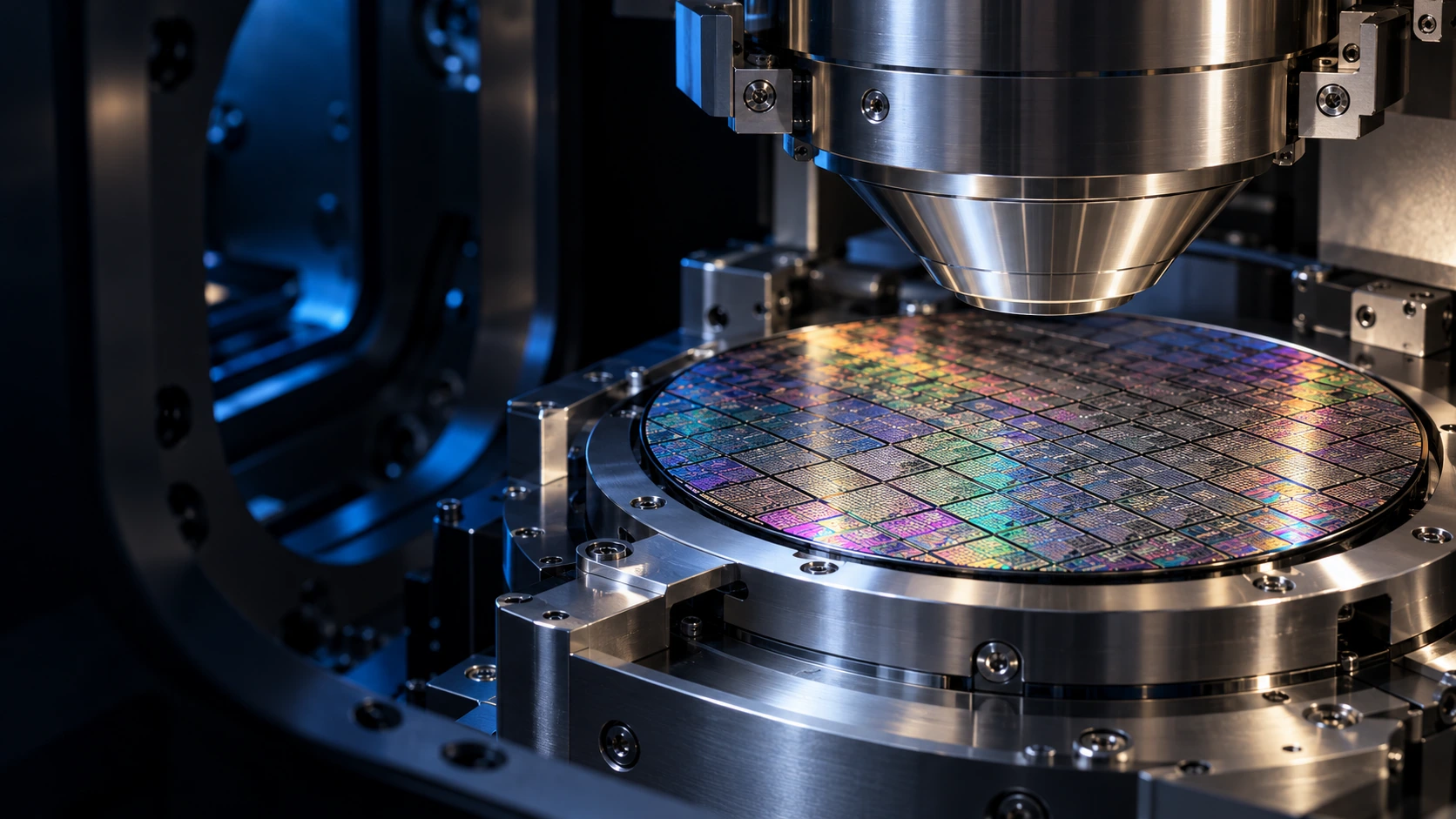
RESEARCH INFRASTRUCTURE
Simulation, fabrication and optoelectronic testing connect materials, structures, devices and application validation.
01 / LABORATORY
Materials preparation, pattern fabrication, characterization and optoelectronic testing support collaborative research.
01Materials Preparation
Material growth and thin-film preparation for micro/nano optical structures.
02Optoelectronic Testing
Electrical characterization and photoresponse testing connect sample preparation with performance evaluation.
03Spectral Analysis
Infrared spectroscopy and microscale analysis for material and device optical properties.
04Micro/Nanofabrication
Local micro/nanofabrication and sample preparation for structural research and process validation.
05Thin-Film Deposition
Functional thin-film deposition supporting material systems, device structures and fabrication workflows.
06Patterning & Characterization
Electron-beam patterning and microstructural imaging for micro/nano pattern development.
07Clean Process Environment
A clean environment for sample preparation, process operations and experimental work.
08Precision Laser Processing
Precision laser processing and cutting for sample preparation and structural fabrication.
02 / METALENS
Simulation, prototyping, imprinting and multiscale characterization of planar focusing lenses, beam-splitting DOEs and spectral filters.
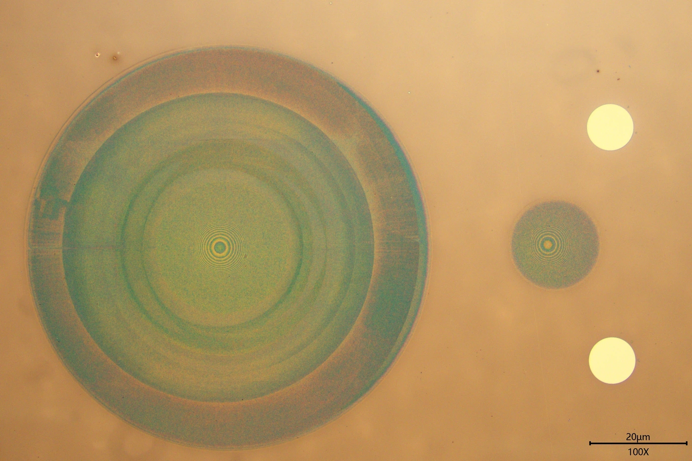
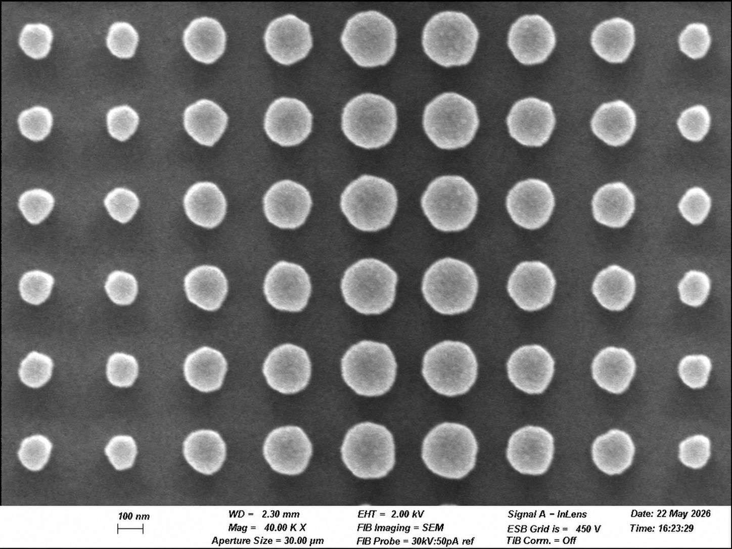
Planar micro/nanostructures for focusing and imaging, with optical microscopy, SEM, samples and test results.
VCSEL-array beam shaping and splitting, from design and samples to measured optical spots.
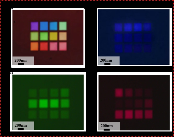
Multichannel spectral control using localized surface plasmon resonance.
CONTACT
Contact us for product selection, development
and project collaboration.
266 Fangzheng Avenue, High-tech Park, Liangjiang New Area, Chongqing, China
Zhongke Yaoguang (Chongqing) Optoelectronics Technology Co., Ltd.RESEARCH FOUNDATION